Scientific instrumentation
Atomic Force Microscope - from Lab to Fab - via Space
The development of an instrument for a specific experiment is very often the first step for exploiting new scientific knowledge and bringing it closer to industrial applications. Fundamental engineering research addresses the hurdles that must be overcome in order to make new insight usable for a larger community. This can be nicely illustrated by the example of the atomic force microscope [AFM]. The instrument was invented in 1986 [1] in the search of a tool that allows imaging insulating surfaces with atomic resolution, comparable to the earlier scanning tunnelling microscope [STM]. At that time, both instruments, the STM and the AFM, were “homebuilt” by the scientists who wanted to use them. But soon start-up companies began building and selling instruments for other scientists who did not have the capacity, knowledge or interest to construct it themselves. Through a close interaction with these expert-costumers, the instruments were constantly improved, which finally opened new applications fields where non-specialists carry out operations.
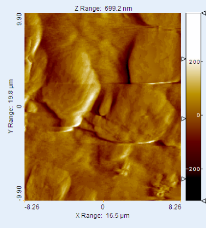
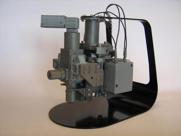
From an instrumentation point of view, one of the most demanding applications on that path was the development of an instrument for planetary science [1] and space research [2]. These instruments needed to be extremely robust and operated in an autonomous mode. Having successfully demonstrated AFM measurements on Mars, see Figure 1, under such special circumstances made the instrument fit for the next challenge: applications in a production line. During the European FP 7 project aim4np [3] we demonstrated such a concept, where innovative sensors, actuators and control technology were combined in a mechatronic solution. This allowed establishing a stiff, virtual link between the instrument and the workpiece while the AFM was mounted on and positioned by a robot. Therefore, the vibrations, which are typical for such an environment, were no longer hindering nanometre-resolution measurements. Figure 2 shows a model of the instrument that was mounted to a robotic arm and successfully operated in an environment that mimicked the vibration of a production line. Future applications could be found, for example, in the production of flat-panel displays, high-precision injection moulding, or role-to-role imprinting of nanopatterns on foils etc.
Microfabricated Tensile Tester - a Tool for Mechanically Probing 2D Materials
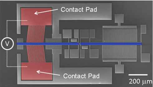
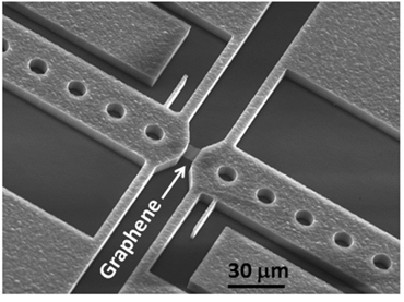
Graphene and other 2D materials are well-known for their attractive electronic characteristics. However, they show also interesting mechanical properties, which were investigated by e.g. atomic force microscope based indentation techniques [5], or by bending a substrate onto which the 2D materials were transferred, and which allowed straining the 2D material [6]. Inspired by earlier work of the group of H. Espinoza, [7] we developed a MEMS tensile tester shown in Figure 3, which allowed straining graphene while measuring at the same time the applied force and investigating the changes in the Raman spectrum. Straining graphene to more 10% was demonstrated using this device [8].This technique is currently further developed such that we can study the changes of interaction of 2D material with surrounding gasses as function of the applied strain.
Research leader Urs Staufer, Professor Mechanical Engineering/Micro and Nano Engineering
References
[1] G. Binnig, C. Quate, and Ch. Gerber, Phys. Rev. Lett. 56
, 930 (1986).
[2] phoenix.lpl.arizona.edu/science_meca.php
T. Akiyama et al Sensors and Actuators
A 91, 321 – 325 (2001).M. Hecht et al Jour. of Geophysical Research - Planets 113
, E00A22 (2008).
[3] sci.esa.int/rosetta/35061-instruments/
W. Barth et al. Microelectronic Engineering
57–58, 825–831 (2001).[4] www.aim4np.eu
[5] Changgu Lee et al, Science 321, 385 (2008).
[6] T. M. G. Mohiuddin et al Phys. Rev. B 79, 205433 (2009).
[7] Y. Zhu et al Appl. Phys. Lett. 86, 013506 (2005)
[8] H.H. Perez Garza et al, Nano Letters 14, 4107 - 4113, (2014); DOI: 10.1021/nl5016848