
Building a lensless microscope to study next-gen chips
Transistors used in computer chips have now reached the tiny scale of mere nanometres, yet chips manufacturers still lack the optical power to study this new generation of chips. Researchers from TU Delft have built a lensless microscope to make an image at the scale of 200 nanometres. With further refining of this technique the researchers expect to bring images of nanoscale transistors within their grasp in the next two years.
With the success of their first test, the researchers found their baseline to fine-tune the lensless microscope towards sharper imagery. The end goal: making even the smallest structures on these chips – the 5 nanometre sized transistors – visible in the next two years. The research project is part of the LINX consortium (Lensless Imaging of 3D Nanostructures with soft X-rays), a collaboration between five Dutch universities and industrial partners such as ASML, a maker of machines used in the production of computer chips.

Sven Weerdenburg
Infrared light, gas and mirrors
Why are regular lenses no longer sufficient to study today’s chips, which hold structures on the nanoscale? PhD researcher Sven Weerdenburg explains: “As a chipmaker, you want to know about all the errors that occur while building your chips so you can improve on them. But you can’t view these chips with conventional microscopes. They work with the wavelength of light visible to the human eye, which is between 400 and 700 nanometres, but you need images with a resolution much higher than 400 nanometres. That’s where lensless imaging comes into play: it works with Extreme Utraviolet (EUV), which has a much shorter wavelength of around 13,5 nanometres.”
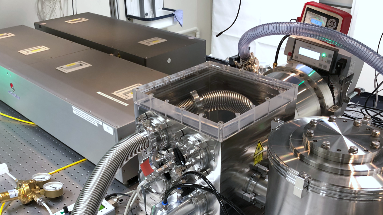
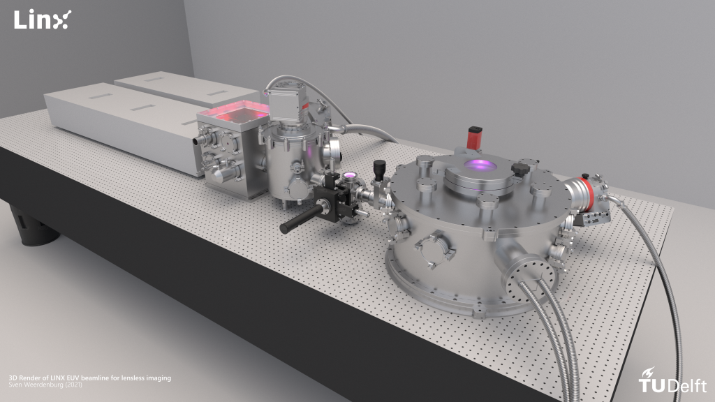
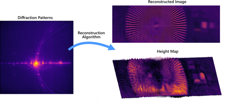
One year ago, the researchers started to build the lensless microscope in cooperation with DEMO, TU Delft’s facility for experimental technical and scientific education: a 5-meter large set-up containing a powerful infrared laser, a giant box to generate EUV light and an imaging chamber. The infrared laser light is focused, then a noble gas is injected into this beam, which starts to emit much shorter wavelengths. Mirrors are used to shape the EUV beam and focus them on a chip sample which scatters the light: this scattering pattern is then captured by a camera in the imaging chamber. Software is needed to translate the scattering patterns into an actual image.
Matching set-up and software
One of the challenges of the project was to make the right match between the set-up and the software to interpret the image, both fraught with uncertainties. Technician Roland Horsten: “Imagine you shine a light on a diamond, which scatters the light. We look at that sparkling pattern. Our colleague Yifeng Shao developed a software which tells us where this sparkling is coming from and how the diamond – in our case the chip – looks like. Since we saw an actual image with this first measurement, we now know the software basically works, and the set-up works as well.” Building the setup, writing the software and producing the first images took the team one year.
Applications for lensless imaging are especially valuable for manufacturers of next-gen computer chips. Weerdenburg: “We imagine that these companies, such as Intel and TSMC can attach such a lensless microscope next to their waferstepper: a kind of printing machine to make the chips. Our device can be used as an inspection tool to see if the waferstepper is doing its work properly. The light we use in our system, with a wavelength of 13,5 nanometres, is the same light these wafersteppers uses to produce these chips. This means we also get a sense of the errors which are only visible in this wavelength, so we can better detect what might be wrong with our sample.”