Photonics for faster Internet
A major challenge in photonics is the accurate alignment of photonic chips, lenses and mirrors that are used in miniscule devices. Researcher Marcel Tichem works on a method to let this part of the assembly take place inside the device itself, known as on-chip assembly. That would make production more accurate and much faster than current manual production processes. A promising application for this novel assembly concept are devices for the transfer of data over fibre optic cables.
Marcel Tichem is an Associate Professor at TU Delft’s department of Precision and Microsystems Engineering (PME). His work is set in the world of high-tech systems, where precision, speed and reliability are of the essence. “Companies like ASM International, NXP, ASML, and FEI create complex, high-performance machines and instruments. We develop new concepts for the control and actuation of precision systems and microsystems, and for automated design”, says Tichem. “Such concepts make it possible to meet the high demands of optical systems: the precision alignment of lenses and mirrors, for example.”
Fibre optic data transfer
One application of Tichem’s work is fibre optic data transfer. The bandwidth of traditional copper-based cable and the amount of data that can be sent are limited, but the demand for data traffic keeps growing. In fact, the explosive growth of online video and mobile data threaten to grind the internet to a halt. Then there is the sustainability factor. “Copper is not very energy-efficient”, he says. “That is why you find these colossal datacentres next to even more colossal cooling systems, often in a port area so enough water for cooling is available.” Using fibre optics could solve both problems. “You can transfer so much more data over fibre optic cable, and it doesn’t produce excess heat.”
“Photonic chips work with light instead of electrical signals. They can detect or generate light waves, change their colour and so on”, explains Tichem. “Such micro-sized structures are very difficult to produce. Imagine, for example, that you have to make a tiny laser source that emits a stable beam and can continue to do so over a lifespan of a few decades.” After years of research, however, The Netherlands are now at the forefront of photonic chip development, and Photonic Integrated Circuits (PICs, the optic version of traditional microchips) can be produced at a reasonable price. But photonics are an order of magnitude more complex than electronics. Photonic devices, called packages, contain micro‐optics and electrical components, as well as PICs.
On-chip MEMS for photonic alignment
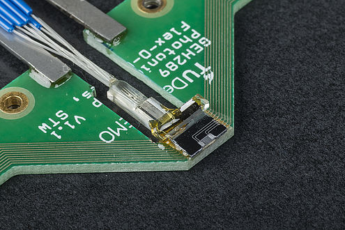
“Such a package is really a complex photonic system. Particularly the integration and alignment of all the parts make the assembly extremely complex, and industry does not have the technology yet to automate this process”, Tichem says. He is working on that though: his current research focusses on microscopic mechanical devices, or MEMS for on-chip photonic alignment. “We are integrating tiny mechanicals systems on the chips, so they can help align their photonic elements.” This research is part of an STW project as well as an EU-funded project PHASTFlex (Photonic Hybrid Assembly Through Flexible Waveguides) that is looking into automated assembly systems in response to the needs of the data communications sector. Within this project, cooperation exists with major European players working on applications and photonic chips (LioniX, Oclaro) and precision assembly (ficonTEC, Aifotec).
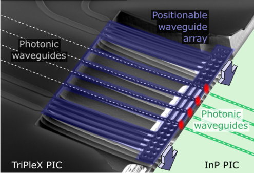
Photo: TJ Peters” Micromachines 2016, 7(11), 200; doi:10.3390/mi7110200
A first achievement on the road towards full automation would be the automatic alignment of two PICs in one package. “In electronics assembly, machines can pick and place thousands of chips per hour. In optical assembly, this is still operator based, using microscopes and precision stages”, says Tichem. Project PHASTFlex is working on a two-step process. First, a machine picks up the PICs and places them on one substrate, with an accuracy of a few micrometres. The machines can do this, but this is still far too inaccurate for perfect alignment. That is the task of the on-chip MEMS. “On one of the chips we integrate an assembly machine consisting of tiny motors, or actuators. With the help of these actuators, you can slightly adjust the position of flexible waveguide beams on one chip in relation to the other.” As the name suggests, the assembly functionality is added solely for the purpose of assembly. “You only use it once. That takes space on your systems, and it costs money, but you have to offset that against current production methods that are labour-intensive.”
PME
The department of Precision and Microsystems Engineering (PME) is one of TU Delft’s departments working on technologies that can be used in optics. PME’s specific mission is to use the phenomena and technologies of the small-scale to create breatrhough innovations of smart materials, systems and devices. “We are mostly involved with mechatronics, meaning systems that have to move very accurately”, says Tichem. “Optics are only one field of application.
Smart materials give new possibilities for improved performance of systems. Tichem explains: “The alignment of mirrors and lenses is critical in optics. However, alignment can change under the influence of temperature fluctuations, for example. You can try and minimise the effects of that by designing a structure, parts of which will not expand under the influence of heat.” That is called topology optimisation, a field that is also important for modern additive manufacturing technology.
Optic technologies – or photonics, the term we use in relation to optical microsystems – are on the rise. Hence, a future chair of the department will focus solely on micro-optics and micromechatronics for photonics. Already the department is developing important enabling technologies. “A lot of what we do here can help others improve optic systems, whether these are medical instruments, inspection cameras or measuring instruments.”
The department PME initiated the NanoEngineering research Initiative (NERI). NERI is a platform for long-term collaboration of industry and academia to jointly turn nanoscience into industrially relevant applications: Moving nano from lab to app.
Moving nano from lab to app requires a new knowledge and technology foundation that allows the development and engineering of repeatable and reliable relevant functions and applications at an industrially relevant scale. This challenge requires cooperative efforts from both industry and academia. PME also takes part in the recently initiated Dutch Optics Center (DOC).