MSc and BSc projects
We are very glad to host you in our group for a BSc/MSc graduation project, internships or another project. We can accommodate students from a variety of programs, including Electrical Engineering, Computer Engineering, Embedded Systems, and (Applied) Physics.
For further information about any project or thesis topic, please contact Fabio or Masoud.
Cryogenic CMOS circuits for quantum computing and quantum sensing (multiple topics)
Quantum computers hold the promise to efficiently solve problems that are intractable by classical computers today, such as large number factorization and simulation of quantum systems, by exploiting quantum phenomena for computation. State-of-the-art solid-state quantum processors must be cooled at cryogenic temperatures to preserve quantum behaviour. In addition, quantum processors require an electronic interface to both control and read out the quantum bits (qubits). Such electronic interface must also operate at cryogenic temperature to enable practical connections to the thousands of qubits envisioned in future quantum computers. The electronic interface spans from the digital to the analog domain and comprises several analog and mixed-signal components, such as data converters, voltage/current references and low-noise amplifiers.
Several projects are typically available, either focusing on a different circuit component or on the characterization of CMOS technology at cryogenic temperature. You will find below a few examples. Please note that those are just examples and more are available: Feel free to come over to discuss your interest! We are also open to adapt the projects also according to a specific interest.
We can tune the project to the needs of your specific program. For instance, we offer both 45-ECTS MSc thesis projects and the combination 15-ECTS internship + 45-ECTS thesis.
Circuit-design projects
The objective of each of the circuit-design projects is the design and implementation of a CMOS analog/mixed-signal circuit component for use in the electronic interface for quantum processors and quantum sensors and operating at cryogenic temperatures close to the quantum devices. While prior works have demonstrated the functionality of CMOS devices at cryogenic temperature, the challenge will be to design circuits operating at temperatures as low as 4 K and below and achieving performance comparable with state-of-the-art designs operating at room temperature.
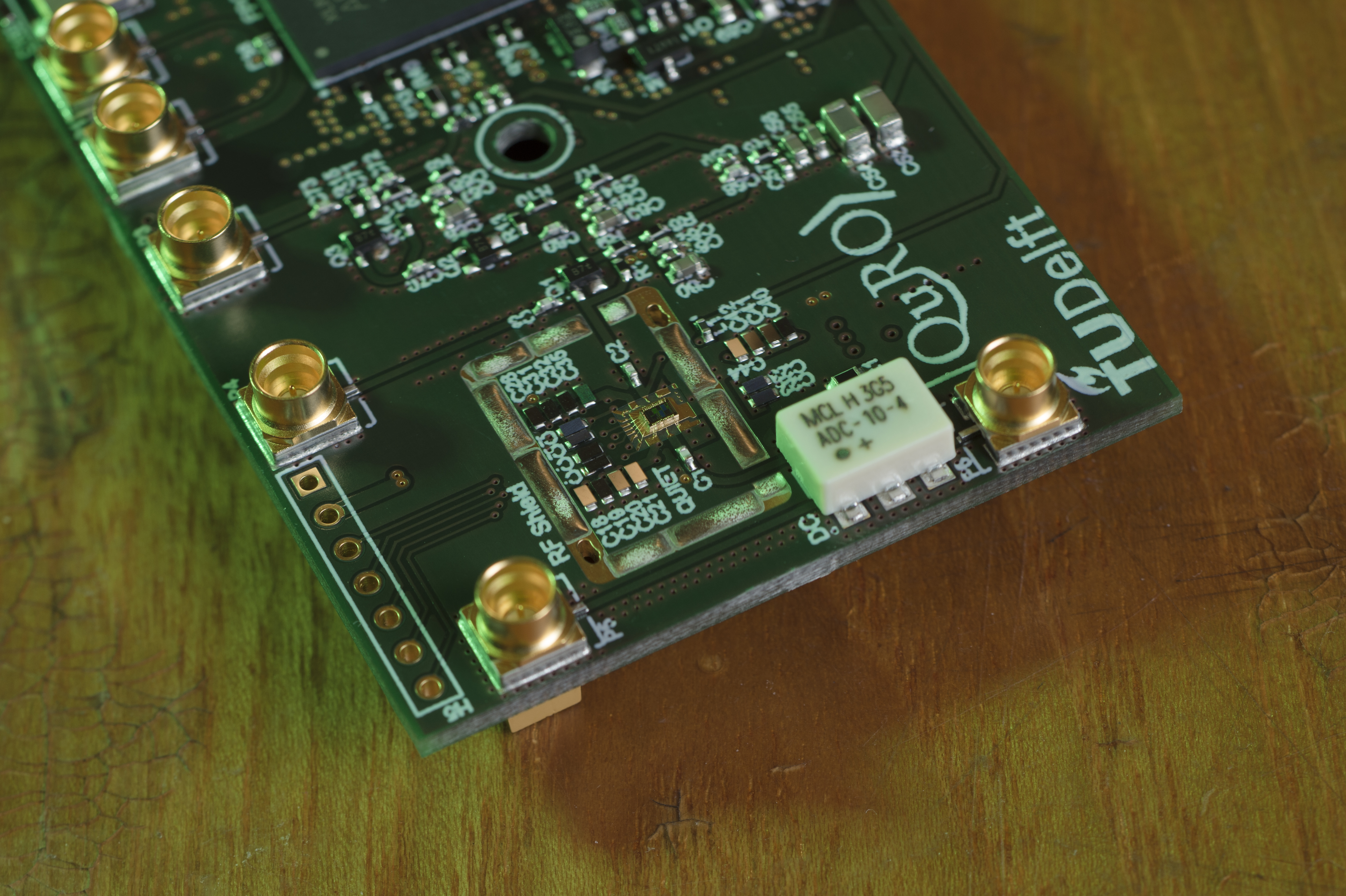
The project will include the circuit design (schematic and layout), the tape-out of the designed circuits (typically in 40-nm or 22-nm CMOS), and characterization of the fabricated circuit. Projects are available in several different areas, including analog, RF, mixed-signal, and digital circuits.
The project will comprise the following phases, partially or fully, depending on execution speed and time constraints:
- Literature review on cryo-CMOS and specific circuit architectures
- System analysis and choice of best architecture
- Circuit design in commercial CMOS process (40-nm CMOS, 22-nm CMOS, SiGe BiCMOS)
- Layout of test chip
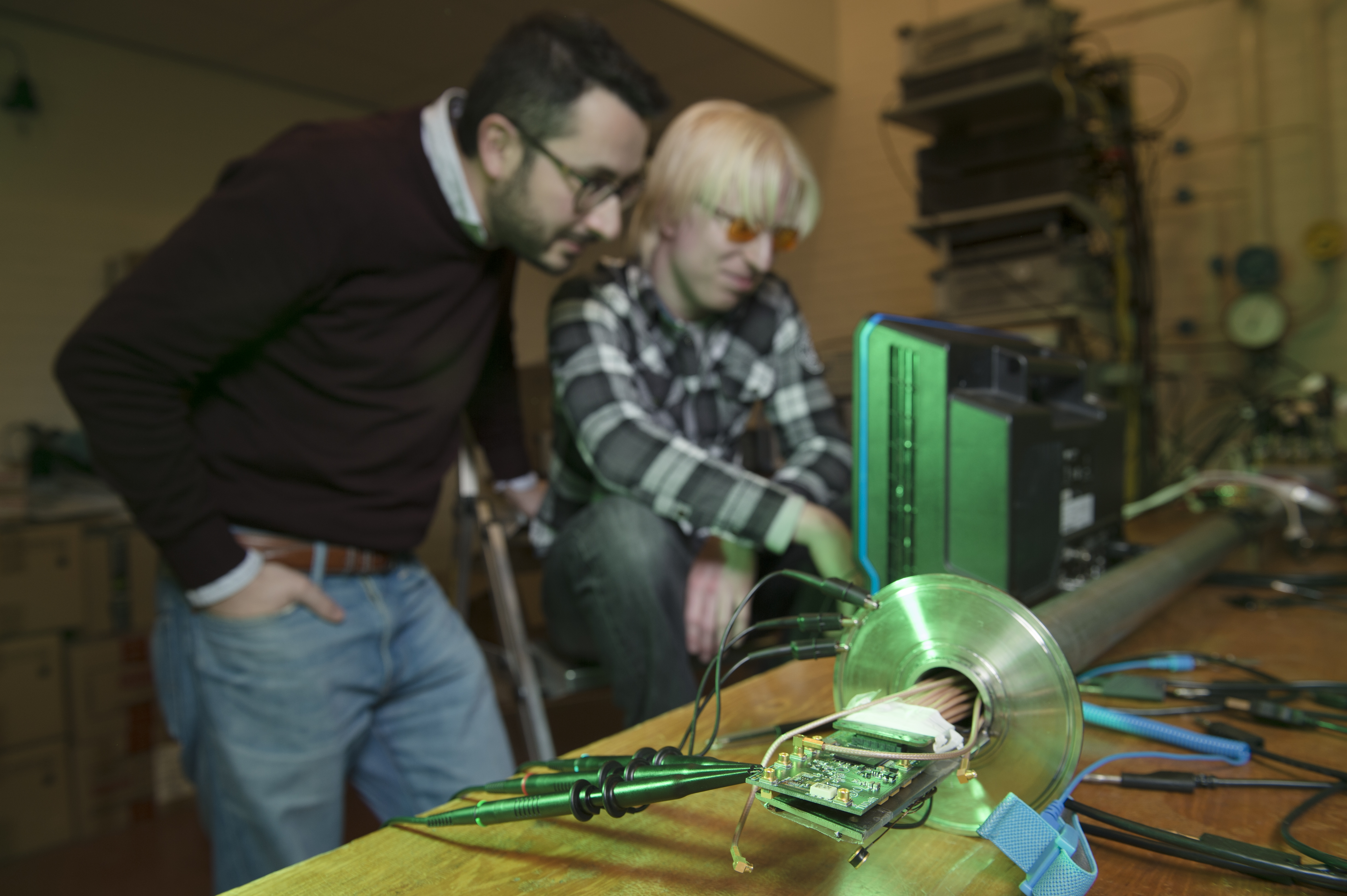
- Preparation of measurement setup (PCB, instrument automation)
- Measurement and analysis of performance
- Writing of report
Cryo-CMOS high-speed analog-to-digital converter
Reading out the state of qubits is accomplished by reading an electrical signal. To minimize the complexity of the wiring between the qubits and the read-out electronics, it is desirable to exploit frequency multiplexing to read out several qubit channels over a wide bandwidth. We have recently built the first cryo-CMOS ADC offering a very high sampling speed, up to 1 GSa/s, and we want to push performance (in terms of bandwidth, resolution and power efficiency) even further.
Cryo-CMOS fast digital-to-analog converters
This project focuses on the implementation of a fast DAC (sample rate above 100 MSa/s) to generate the very fast voltage pulses required to implement two-qubit operation in solid-state quantum processors.
Cryo-CMOS temperature sensor
What is the best way to sense temperature down to 4 K and below using standard CMOS technology? In this project, you will push the boundary of existing sensors well beyond the state-of-the-art. Temperature sensing is becoming more and more important for any cryo-CMOS complex circuit, as self-heating plays a fundamental role in the performance of integrated circuits. While you could tolerate a temperature increase of 20 °C at room temperature, an increase of 20 K around a base temperature of 4 K represents a 5x increase in absolute temperature!
SiGe BiCMOS readout for Superconducting Nanowire Single-Photon Detectors (SNSPD)
SNSPDs achieve extremely good performance as optical detectors but need to operate at cryogenic temperature. Routing their outputs to the room-temperature electronics limits the number of sensors that can be placed in a sensing array. In this project, you will design a SiGe BiCMOS low-noise amplifier that exploits the cryogenic performance of SiGe bipolars to bring the readout as close as possible to the detectors.
Cryo-CMOS Time-to-Digital Converter (TDC) readout for Superconducting Nanowire Single-Photon Detectors (SNSPD)
SNSPDs achieve extremely good performance as optical detectors but need to operate at cryogenic
temperature. Routing their outputs to the room-temperature electronics limit the number of sensors that can be placed in a sensing array. In this project, you will design a cryo-CMOS TDC that can be placed as close as possible to the detectors to measure the time of arrival of the photons.
Cryo-CMOS transimpedance amplifer (TIA) for noise characterization
Characterizing the noise of a single device at 4 K is extremely challenging due to the very long interconnect to the instruments at room temperature. To address this issue, this project targets the design of an ultra-low-noise TIA implemented in a CMOS process and operating at 4 K and below.
Cryo-CMOS Low-noise-amplifier with integrated supply regulator
We have recently demonstrated the operation of cryo-CMOS LNAs for spin-qubit readout. However, those LNAs suffer from poor-supply rejection and must be redesigned in combination with an LDO to provide proper functionality. This project will involve the full redesign of the LNA and its co-design with an LDO capable of improving the supply rejection. This is a fundamental step to enable the integration of several circuit blocks into a large SoC as required to implement the electronic controller for a large-scale quantum computer.
Cryogenic digital circuits
Building a computing device such as a quantum computer requires a large amount of classical logic, for instance to provide hardware support for the quantum microarchitecture and to process the digital signals from and to the data converters directly connected to the quantum processor. In this project, the objective is to exploit the specific advantages of cryo-CMOS devices, such as the extreme low leakage and the high-subthreshold slope, to design logic circuits, such as memories and/or combinational logic, with superior performance, in terms of speed and/or power efficiency,
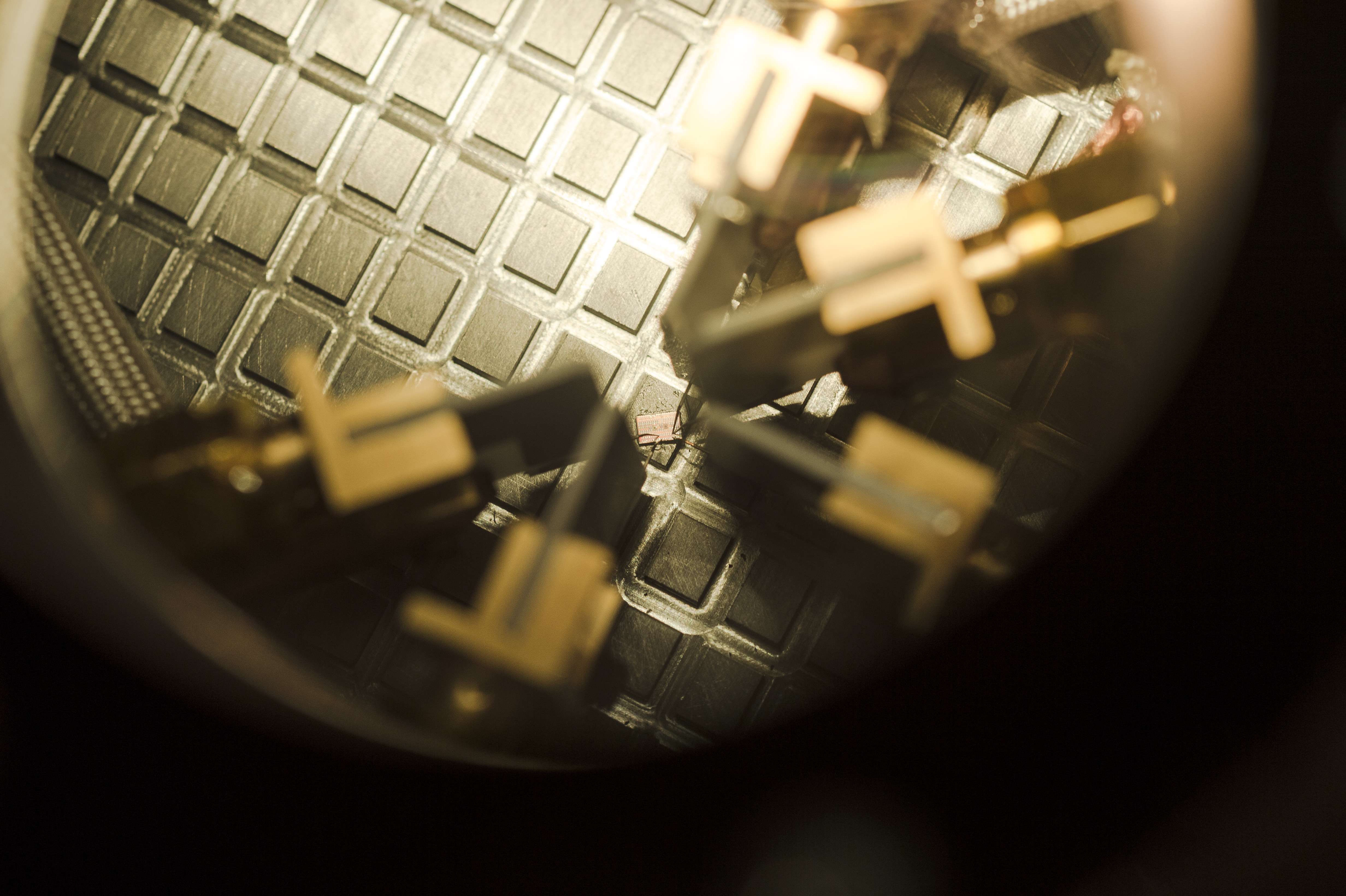
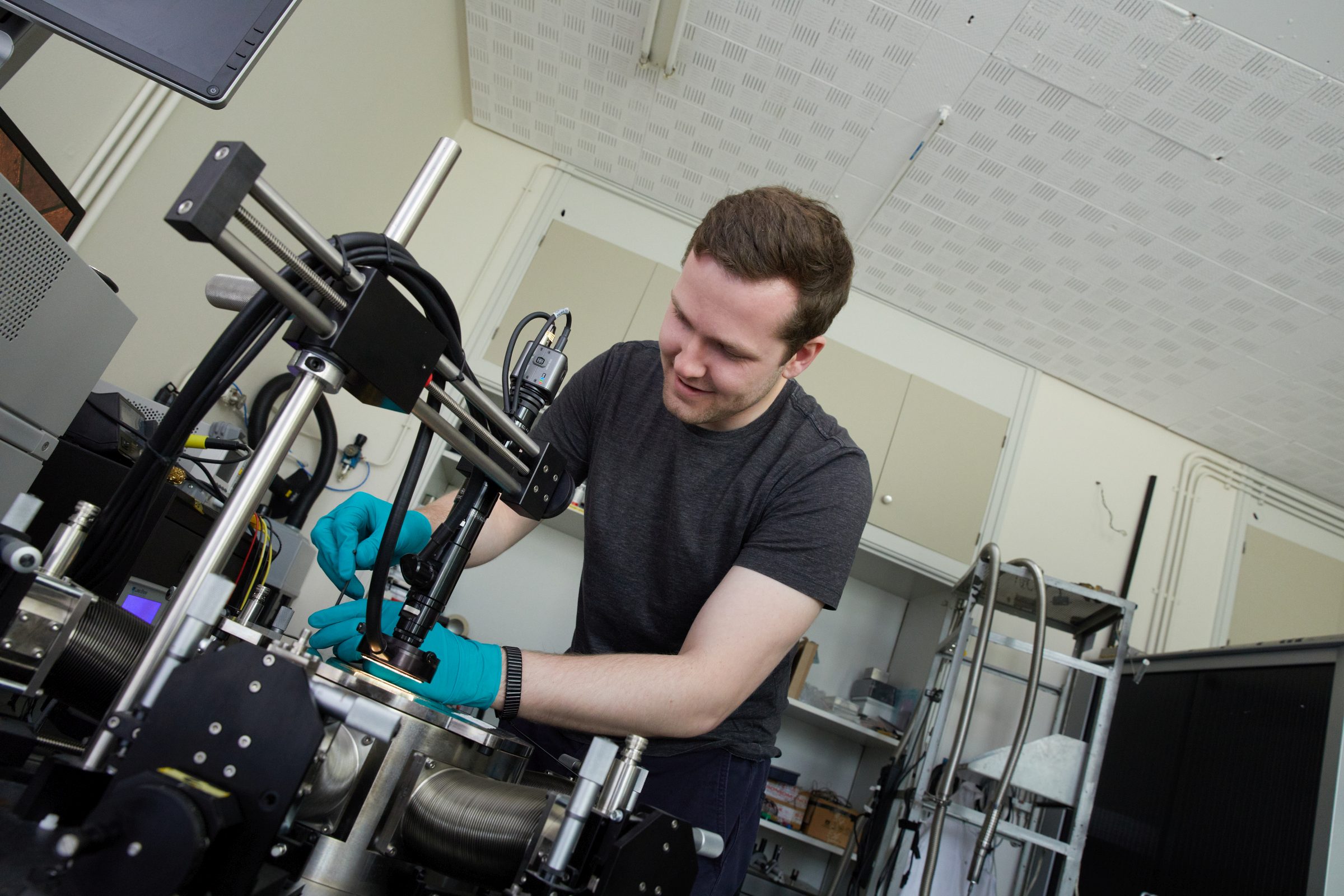
Characterization-oriented process
The aim is to characterize devices from several CMOS technologies over a wide range of cryogenic temperatures (30 mK – 77 K) and develop models suitable for analog and digital circuit design over such a range. Currently, we have already fabricated and characterized test structures in 0.16-μm CMOS and 40-nm CMOS and, in collaboration with Prof. A. Valdimirescu (UC Berkeley), we have been able to build a device model that is compatible with standard integrated-circuit design tools and that has been used for successfully designing complex analog circuits. But the road towards a full-fetched device model is still long, and there are many interesting physical effects to be investigated, both from the point of view of characterization and form the point of view of moelling.
CMOS operation at cryogenic temperature and in large magnetic field
Spin quantum bits (qubits) require operation at sub-K temeperature and in the presence of a large magnetic field up to a few Tesla. Since the neighboring cryo-CMOS electronics will be subject to the same conditions, this project aims at characterizing CMOS transistors in those conditions to understand the device behavior and build a device model usable for circuit design.
Noise in cryogenic CMOS transistors
Circuit characterization points to the linear temperature scaling of thermal noise in CMOS transistors not holding down to cryogenic temperature. To understand the device behavior at 4 K and below, this project focuses on characterizing noise from very low frequency (< 10 Hz) to moderately high frequency (> 10 MHz).
Cryo-CMOS models
In this project, we aim at characterizing and modelling the electrical behavior of CMOS devices, such as transistors and passive devices (inductors, capacitors, resistors) over a wide range of temperatures from 4 K to 300 K. We already have the availability of a very large number of test structures ready for cryogenic characterization, which can be followed by data analysis, physical modelling and embedding of the developed models in a compact simulation model to be used for circuit design. If you are an electrical engineer or a physics student with love for experimental work and passion for the physics aspects of our discipline, this is the project for you!