Design and implementation of photonic routes for efficient delivery & collection of light from NV centers in diamond for biosensing Header Slider
NV-centers in diamond are very promising candidates when it comes to sensing very small magnetic fields. Taking this one step further, we can use this system in order to perform sensing of bio-samples, such as detection of a magnetic footprint caused by cancerous cells.
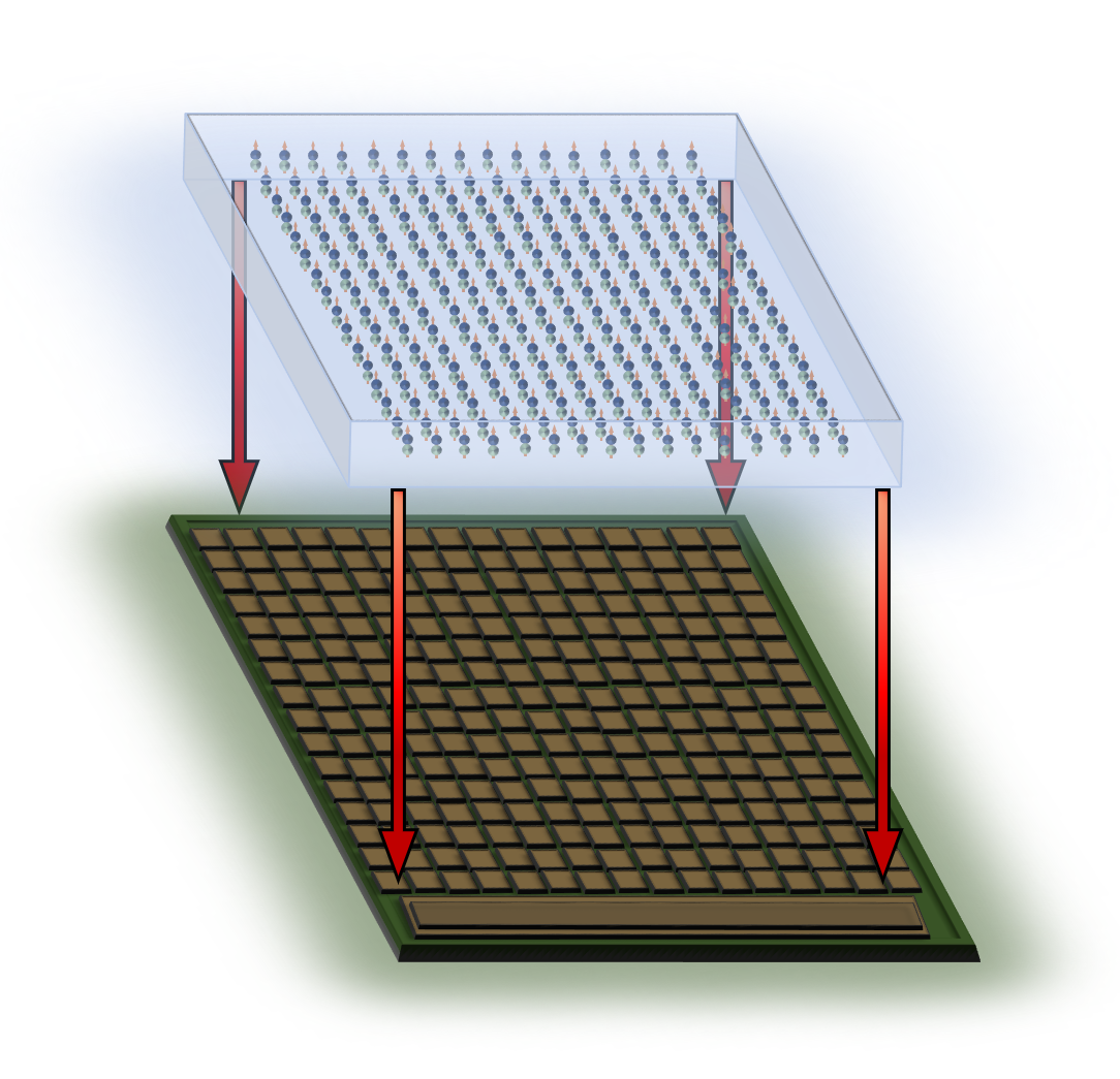
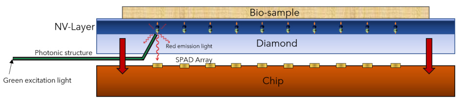
Whereas most setups utilizing NV-centers in diamond operate in a lab environment using optics and bulky equipment (photodetectors), we aim to bring the sensing component of this system down to a chip level. For this reason, a diamond substrate with deterministically implanted NV-centers will be fabricated and integrated into a CMOS chip along with an array of Single-Photon Avalanche Diodes (SPADs), positioned so that they can efficiently collect the light emitted from the single NV centers in the diamond, providing an increase to the platforms sensitivity and creating a small and compact biosensor.
However, when dealing with bio-samples, it is imperative to avoid direct excitation of the bio-sample itself. The excitation light must be accurately steered and directed towards each NV-center located in the NV-layer of the diamond itself.
Project goal:
- To design and fabricate a photonic structure/waveguide which will then be integrated into the chip containing the diamond and the photodetectors.
- Characterization of the fabricated waveguide.
This structure must take into account:
- An efficient design of the photonic structure itself
- An efficient route to drive the excitation light into the NV centers, without exciting the bio-sample
- Filtering of unnecessary light emissions & reflections
- Operational parameters of the SPAD (cross-talk)
The fabrication part of this project will be carried out in the cleanroom.