Semiconductor nanocrystals
Positrons as sensitive probe particles for the surfaces of colloidal semiconductor nanocrystals for future thin film solar cell
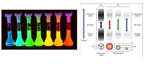
Size and Color
Fundamental properties of semiconductors such as their melting temperatures, optical bandgap and local crystal geometry, may vary substantially with the particle size below ~10 nm. This is directly visible from the clear changes in color of solutions of mono-disperse colloidal CdSe nanocrystals with different sizes (Fig. 1). These effects arise from the confinement of electrons and excitons within the finite size of the quantum dot. The resulting large tunability in optical properties can be used to create innovative light-emitting diodes and thin film solar cell devices.
The positron as a new, strongly needed probe for surfaces of nanoparticles
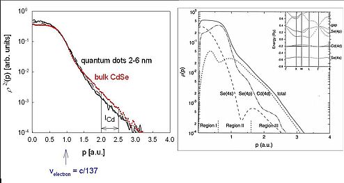
New insight in these properties can be obtained by using the positron – the anti-particle of the electron – as probe particle. Positron beam experiments provide information about the electron momentum density ρ(p) (EMD) of valence electrons of the studied material (see Figure 2 for CdSe).
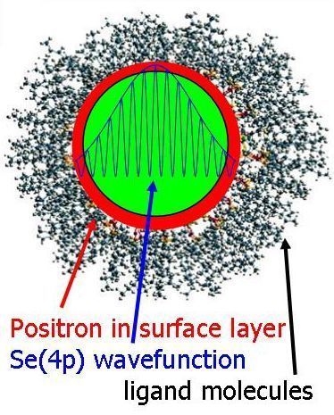
Our recent studies on thin films of CdSe nanocrystals show that the positron effectively traps at the surfaces of the nanocrystals in a shell-like surface state (Fig. 3) [1]. Comparison of the curves in Fig. 2 extracted from positron 2D-ACAR distributions with that of bulk CdSe shows a reduction in annihilations from Cd semi-core electrons in the nanocrystals, indicating that positrons annihilate mostly with Se electrons in the surface layer. This provided unambiguous experimental confirmation of the strong outward relaxation of Se atoms at the nanocrystal surfaces, predicted by first-principles calculations at Lawrence Livermore National Laboratory [2].
This new way of looking at the surfaces of nanocrystals is very promising. For progress in applications, control over surface processes and surface composition of nanocrystals is of vital importance. The surfaces play a key role in catalytic activity, and in the mechanism of doping nanocrystals [3]. Furthermore, when considering optical applications such as solar cells, the unwanted non-radiative recombination of electrons and holes at the surfaces may be reduced by tailoring the surfaces.
The special merit of the positron method is its ability to measure depth profiles of films in the sub-micron range (between 10 nm and 2 μm) in a non-destructive manner. Promising areas of application therefore include ultra-thin solar cells [4], metal hydride nanocrystals for improved hydrogen storage, and semiconductor quantum dots or wires for opto-electronic applications.
Key Publications:
- [1] S.W.H. Eijt, A. van Veen, H. Schut, P.E. Mijnarends, A. B. Denison, B. Barbiellini, A. Bansil, Nature Materials 5, 23-26 (2006).
- [2] A. Puzder, A.J. Williamson, F. Gygi, G. Galli, Phys. Rev. Lett. 92, 217401 (2004).
- [3] S.C. Erwin, L. Zhu, M.I. Haftel, A.L. Elfros, T.A. Kennedy, D.J. Norris, Nature 436, 91-94 (2005).
- [4] I. Gur, N.A. Fromer, M.L. Geier, A.P. Alivisatos, Science 310, 462-465 (2005).
Positron 2D-ACAR with the intense POSH beam at RID
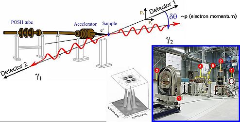
The positron two-dimensional Angular Correlation of Annihilation Radiation (2D-ACAR) method provides the most detailed insight in the electronic structure by a two-dimensional image of the electron momentum density ρ(p). The method is based on detection of the small angular deviations (θx, θy) in 180o emission of the gamma quanta (Fig. 4), which are linear proportional to the momentum p of the annihilating electron.

dr. S.W.H. Eijt (Stephan)
- +31 (0)15 2789053
- S.W.H.Eijt@tudelft.nl
-
Room: 2.01.340