Services
Services
Self Service
You can use our laboratories and equipment. You need a safety training and equipment/process training.
Foundry Services
We can do the processing for you. Our facilities can only be used for prototyping and small scale production.
Joint Development Services
You can use our extensive expertise to do process research, development and manufacturing.
Contact: Paolo M. Sberna
Request for quotation: click here
Process Flow Development
We can help you with the transfer of your idea into a processing flowchart. We will give suggestions, potential solutions, and we will try to use as much as possible standardized EKL process steps to increase the chance of success.
Contact: info@EKL.tudelft.nl
Non IC-compatible Materials
For non-IC compatible materials we have a Process Approval Committee (PAC). Contamination of our standard process line must be prevented and for most materials workarounds have been developed.
Contact: info@EKL.tudelft.nl
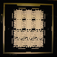
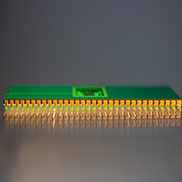
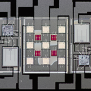
Processes
IC processing line with Bipolar/CMOS capability (1um)
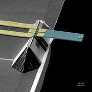
MEMS processing
Bulk/Surface micromachining
Deep Reactive Ion Etching for 3D structures
Through Silicon Vias for 3D integration
Glass Processing
Polymer Processing
Wafer bonding
SUEX: 500 um photosentive laminate
Nano-copper process
- Baseline process for Bicmos, 7 masks with NMOS, PMOS, NPN and PNP (2 um)
- Baseline for c-Si solar cells (19% efficiency)
- Baseline process for nano-reactors
- Baseline process for EUV detectors
Contact: info@EKL.tudelft.nl