ADEM
Silicon nanocrystals embedded in a high band gap silicon alloy are interesting candidates for top cells of multi-junction solar-cells of which the band gap can be tuned by the nanocrystal size. The ability to tune the material's band gap allows us to minimize thermalization losses and thereby increase the solar-cell efficiency. The mean nanocrystal size and size distribution are crucial parameters in determining the optical properties of the material, and electronic transport properties in photovoltaic devices. The project goals are to study the fabrication, characterization and incorporation of embedded silicon nanocrystals into devices.
Research objective
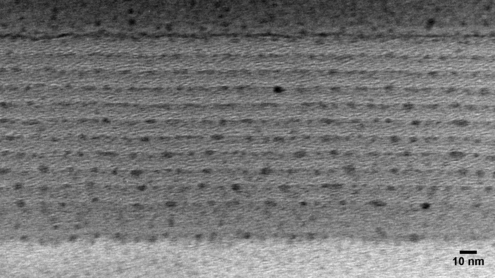
We have developed a method to quickly detect and measure nanocrystals in a TEM image to obtain the nanocrystal size distribution with minimum user input [2]. We compared the accuracy and speed of this method with other methods used in literature and the proposed method performed comparable or better in the image test set.
Furthermore, we have developed an analytical correction for the effect of slicing nanocrystals during transmission electron microscopy sample preparation on the apparent nanocrystal size distribution [2]. This equation can be used to fit a real nanocrystal size distribution from a measured apparent size distribution.
We have also developed a non-destructive measurement and simple analysis method for obtaining the absorption coefficient of silicon nanocrystals embedded in an amorphous matrix [3]. Furthermore, we proposed a model to extract the optical properties and the density of states of both the nanocrystals and their embedded matrix [3].
Publications
- Y. V. Aulin, M. van Sebille, M. Moes, F. C. Grozema, Photochemical upconversion in metal-based octaethyl porphyrin-diphenylanthracene systems, RSC Advances 5, 107896–107903 (2015)
- M. van Sebille, L. J. P. van der Maaten, L. Xie, K. Jarolimek, R. Santbergen, R. A. C. M. M. van Swaaij, K. Leifer, M. Zeman, Nanocrystal size distribution analysis from transmission electron microscopy images, Nanoscale 7, 20593–20606 (2015)
- M. van Sebille, R. A. Vasudevan, R. J. Lancee, R. A. C. M. M. van Swaaij, M. Zeman, Optical characterization and density of states determination of silicon nanocrystals embedded in amorphous silicon based matrix, Journal of Physics D: Applied Physics 48, 325302 (2015)
- D. Deligiannis, S. Alivizatos, A. Ingenito, D. Zhang, M. van Sebille, R. A. C. M. M. van Swaaij, M. Zeman, Wet-chemical Treatment for Improved Surface Passivation of Textured Silicon Heterojunction Solar Cells, Energy Procedia 55, 197–202 (2014)
- P. Babal, H. Lopez, L. Xie, B. van Veen, M. van Sebille, H. Tan, M. Zeman, A. H. M. Smets, Nanostructure Analysis of P-Doped Nanocrystalline Silicon Oxide, 28th European Photovoltaic Solar Energy Conference and Exhibition 2580–2587 (2013)
ADEM
Subsidy:
Duration:
People involved: Dr. René van Swaaij, Martijn van Sebille (PhD candidate), Adele Fusi, Jim Quik, Jort Allebrandi

