Kavli Nanolab News no.15
Cleanroom messages
- Maintenance week: July 11-15 (week 28): CR not accessible for processing
- Functions in TU 7,8 and 10 (rooms P00.360, 340 and 321) will be re-organized. The aim is to create logical split between areas for storage of substrates and consumables and areas for processing and inspection.
Safety

Emergency buttons
In case of chemical spill that is potentially dangerous for you or for other cleanroom users always use the emergency buttons (yellow).Nanolab NL
NanoLabNL will invest firmly in its research facilities in the coming years. This week, the Dutch Ministry of Economic Affairs confirmed a financial contribution to the activities of NanoLabNL, as part of the so-called Toekomstfonds (Future Fund). The Dutch national facility for nanotechnological research will use the acquired resources to stimulate the development of proof-of-concepts, demonstrators and small scale production. The total investment sums up to 13,5 million euros, with 50 per cent covered by the NanoLabNL partners and the other half being invested from the Toekomstfonds. The investments appear crucial for future nanotechnological research activities, including new materials, photonics, quantum technology, nanoelectronics, and micro fluids.
For more information: http://www.nanolabnl.nl/news/nanolab-nl
Equipment
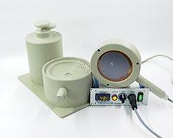
We recently acquired a new tool from Idonus for HF vapour etching. It will be installed in wet bench TU3.1. It an be used for sacrificial etching of silicondioxide without the risk of sticking of released structures by surface tension as in the case of using liquids.
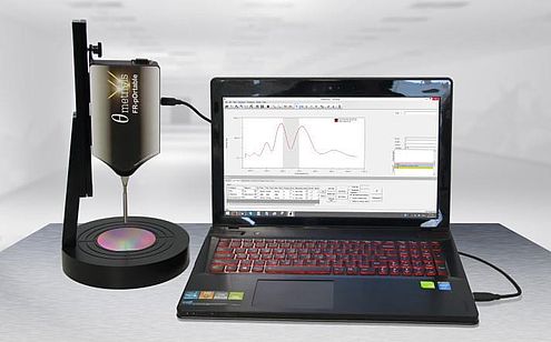
We purchased a ThetaMetris FR-pOrtable measurement system for accurate and precise optical characterization of transparent and semi-transparent single films or stack of films. With FR-pOrtable the user can perform reflectance measurements for films in the 350-1000nm spectral range.
The tool is installed next to the optical microscopes in TU2.
- Ion Beam Etcher: installation of SCIA Ion Mill 150 in September 2016.
- Atomic Layer Deposition: assessment of the tender has been finalized. Provisional awarding will be published on July 5.
- Dual Beam (FIB/SEM): requirements and wishes are written down
- Deep Si etching: market consultation for a combined Cryo – Bosch etcher
We are currently investigating the use of megasonics instead of ultrasonics for more efficient lift-off processing of nanostructures. The technique is quite expensive but we will purchase a set-up if we are confident about its capabilities. If you already have experience please let us know.