
Project details
Semiconductor
Chips are the most indispensable elements of any electronic apparatus, including computers and smartphones. They have a vast influence on our daily life and our means of communication. Advanced networks (5G), personalized healthcare, sustainable cars, the internet of things, and artificial intelligence are all developments that require not only more chips but also more powerful chips.
Chips are composed of many tiny semiconductor components. The fabrication of these semiconductor components happens in dedicated factories and consists of several steps, including lithography, etching, and deposition of thin layers. To make more powerful chips, more of these components have to fit in the same volume and thus in the factories, people try to make smaller and smaller components and conduct the manufacturing steps at ever smaller dimensions.
Imaging during fabrication of the semiconductor components is essential for making them smaller and thus more powerful. Also, imaging is essential to control the quality of the manufacturing process and thus prevent wasting resources during fabrication. Imaging after manufacturing steps like lithography or etching is called metrology, while imaging of the end products is called inspection. As the components on the chips are becoming smaller and smaller, the metrology and inspection techniques need to resolve smaller and smaller details. This puts very strong requirements on these techniques in terms of speed, accuracy, and precision.
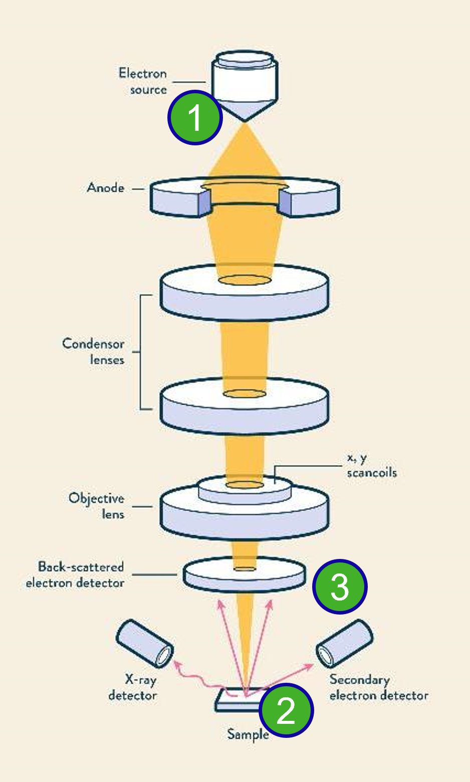
Electron beam microscopy is the imaging technology that can deliver the highest possible resolution. Development of electron beam inspection and metrology is thus essential for process and quality control of semiconductor components for chips manufacturing.
Goal of the project
Improve reliability resolution, and acquisition speed at low landing energies, low contamination and damage levels
With the ever-shrinking device dimensions, the quest for solutions that increase throughput at higher resolution and better image quality continues to be very challenging. Reliable imaging at lower beam landing energies and low contamination and damage levels at high throughput is a must. This calls for a study of the fundamentals of electron beam imaging under these conditions. In addition, these fundamentals have to be translated in an integral system design for an inspection and metrology tool.
In this program, TU Delft, ARCNL, and ASML, join forces in a 5-year program on an integral approach to tackle critical issues in the application of electron beam imaging for semiconductor device inspection and metrology throughout the entire instrument/signal chain: from system design, beam generation and probe formation, via electron-target interaction, signal generation, and image interpretation to extraction of information.
Our research plan is divided in three interconnected work packages that each target a different aspect of the electron image formation process for low-keV electron landing energies: instrumentation, electron-target interaction, and signal generation and detection.
Three research lines:
Instrumentation
- Applications requirements & research into SEM design
- Ultraclean vacuum (mini) environment
- Application-optimized SEM instrumentation (sources, corrector)
Electron-target interaction, with focus on low landing energy
- Simulation models on charging & damage
- Experimental characterization on electron-induced damage & charge diffusion
Signal generation and detection
- Artefact and charging damage removal
- Novel detector concepts
- Experimental validation: the holistic approach
Work packages
-
Acquisition speed is currently limited by the 1 nA current that can be maximally obtained in a nanometer-sized probe. This is a result of both a physical limit of the reduced brightness of electron sources and, for low keV electron landing energies, the need to limit the beam opening angle to minimize aberrations.
Research topics include i) clarification of application-specific requirements and relate those to SEM design improvements, ii) mitigation of sample contamination by active control over vacuum and sample cleanliness and iii) novel concepts and techniques for low-keV aberration correction and for higher brightness sources.
-
We are fundamentally limited by the lack of knowledge of electron-matter interactions. This prevents disentangling the different scattering processes, in space and in physical origin, that contribute to detected signals. This may lead to artefacts and ‘useless’ exposures.
Research topics include: i) refinement of current simulation models of electron-matter interaction and inclusion of models for charging, charge migration and sample damage, ii) predict the contribution of sample charging and electron-induced sample modification and experimental work to measure charging, charge migration and sample damage iii) compare light-induced damage (including heating) with that imposed by electrons.
-
Charging of the sample and modification due to electrons give rise to image artefacts that hamper extraction of reliable and high-resolution information. Effects include local shrinkage of resist, knock on damage, charge field build up, local heating (expansion)
Research topics include i) strategies to prevent image artefacts or to mitigate their effects during scanning and acquisition, ii) use of additional information and signals to discern and mitigate charging effects and explore the design of novel detector concepts for efficient, content-specific signal detection, iii) integrate all findings of this work package with work packages 1 and 2 and perform integral experiments on industry-relevant samples.