Interfaces
Surface and Interface Engineering consists of two research lines with a focus on the effect of interfaces on properties and stability, one conducted by Dr. Wim Sloof and his group and one conducted by Dr. Amarante Böttger and her group. Both associate professors also lead advanced experimental facilities for materials study, an X-ray Laboratory (Böttger) and a Surface Analysis Lab (Sloof).
The program involves both state-of-the-art experimental and theoretical/computational work. The research focuses on subjects that are positioned at the crossroads of scientific challenge, engineering complexity, and societal urgency. Energy applications, self-healing materials, and fabrication techniques for new-generation integrated circuits are the primary subjects.
Publications
The research by Dr. Böttger’s group primarily focuses on surface and interface driven solid-state reactions in solar, hydrogen, and other energy applications. Both experimental and computational methods are used. The research addresses a variety of subjects including metal-hydrogen interaction, silicon-metal compounds and photovoltaic cell materials. In addition, new techniques are developed for X-ray diffraction and fluorescence experiments, also involving advanced statistical analysis of diffraction data.
The X-ray Laboratory has state-of-the-art XRD and XRF equipment. The research is focused on powder diffraction, texture analysis, strain and defect density determination and, where XRD and XRF combine, on composition analysis.
The mission of the lab is to supply high precision, high reliability data for our own research projects, and for researchers in and outside the department, several of them across TU Delft. External companies and governmental organisations also make use of the group’s expertise.
Research
The research primarily focuses on surface and interface driven solid-state reactions and their role on performance and lifetime. The overall goal is to design materials for hydrogen and solar energy applications, and industrial products with improved performance and lifetime. Topics studied are microstructural and compositional effects in metal-gas interaction, hydrogen purification, phase stability, high-entropy alloys and silicon-metal compounds. In-situ analysis of materials using advanced experimental facilities for structure and surface analysis, and statistical thermodynamic calculations.
Lab facilities
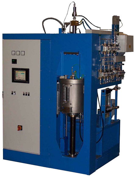
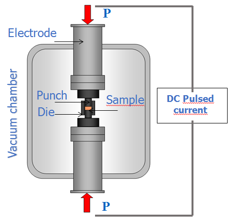
Spark Plasma Sintering for synthesis of advanced materials
Spark Plasma Sintering (SPS) is a versatile technique to synthesis a variety of materials, ranging from polymers, metals (alloys and intermetallics), ceramics and composites. Pure powders are mixed in the desired composition and compacted in a graphite mould. In vacuum, but with the powder mixture under pressure and applying a pulsed current, the mould is heated and the material sintered. It is believed that plasma is created that enhances the sintering process. This modern sintering technology allows manufacturing of all kind of materials at lower temperatures and pressures than the traditional manufacturing methods. Moreover, it has been proven that materials, which are difficult or even impossible to prepare by traditional techniques, can be manufactured by spark plasma sintering. For example, Ti and Zr alloys, Mo intermetallics and magnetic materials.
Precision Annealing, Oxidation and Reduction Furnaces for materials processing
Thermal Analysis Apparatus
For studying surface and interface reaction as well as gas-solid interactions at elevated temperatures and in different environments the following methods are used:
- Thermogravimetric Analysis (TGA)
- Differential Thermal Analysis (DTA)
- Differential Scanning Calorimetry (DSC)
Thin film and coating deposition
Leica
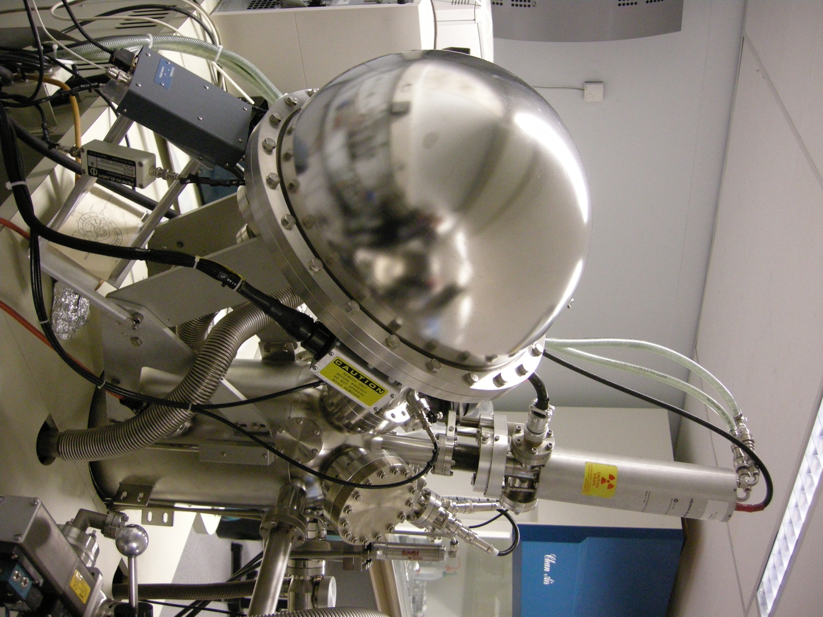
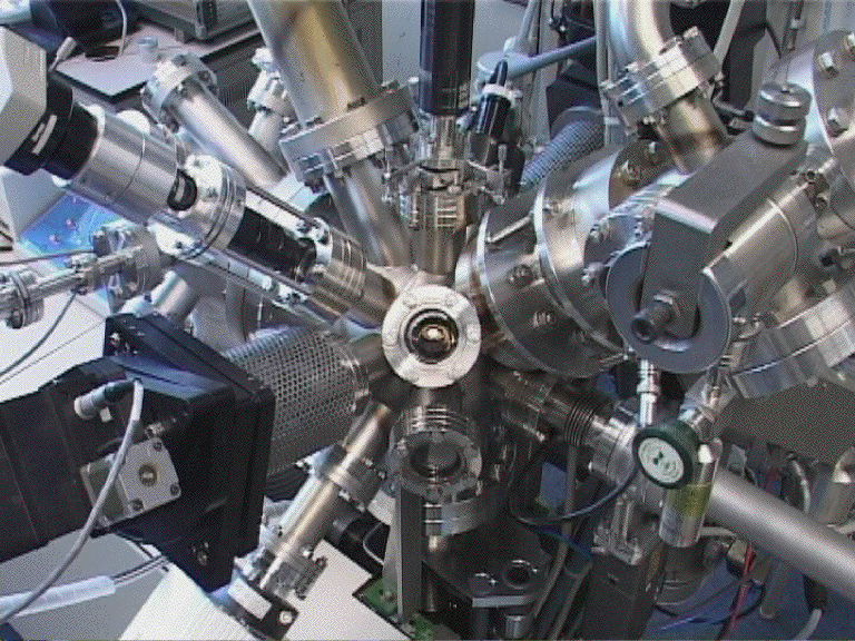
The UHV processing chamber is developed to study surface reactions, element segregation, oxidation and reduction. Samples can be heated up to 1000 °C. Their surface can be cleaned with atomic hydrogen or argon ion sputtering. This facility is equipped with mass spectrometer to analyse and control the gas composition in the recipient. Also, a variable wavelength ellipsometer for in-situ monitoring thin film growth is present. Further, thin films can be deposited with an evaporator. The vacuum system is divided into three separate compartments: (i) a main processing chamber, (ii) a chamber for gas analysis and partial pressure regulation, and (iii) a chamber for evaporation of metals. The chamber is coupled to analysis chamber to transfer the sample for XPS,AES, ISS and LEED analysis.
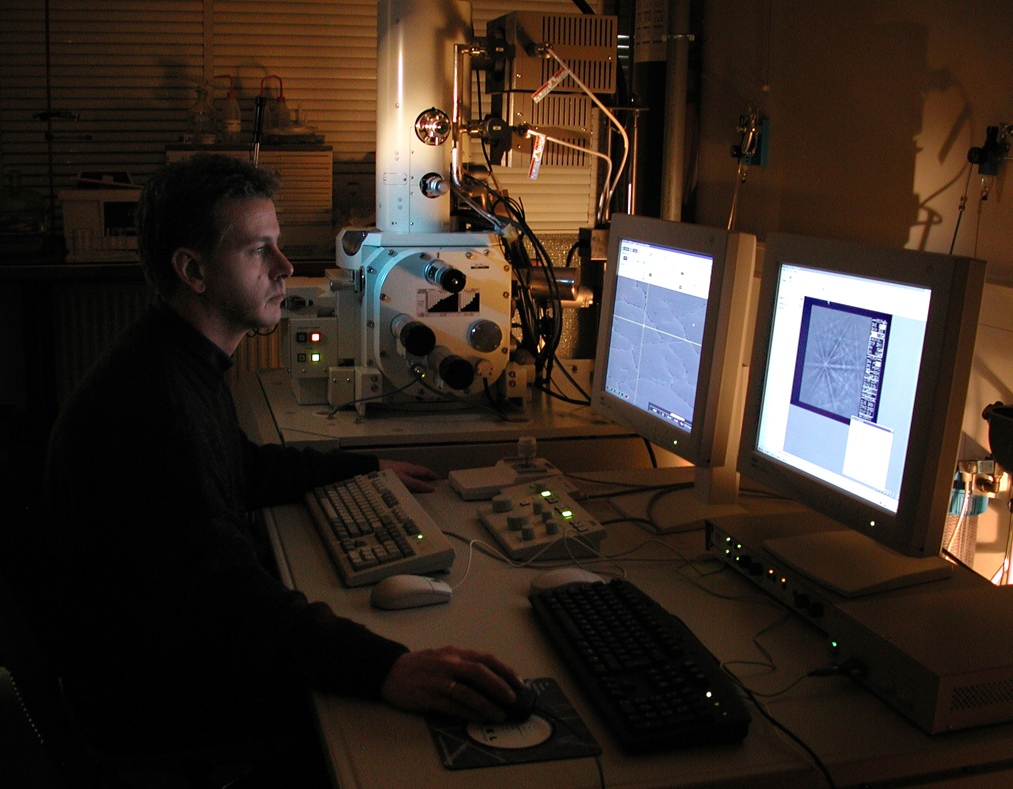
Scanning Electron Microscope, SEM (JEOL JSM 6500 F) equipped with a field emission gun and provided with a large specimen analysis chamber. This microscope is also equipped with an energy-dispersive X-ray microanalysis (XMA) system (Noran System 7, Thermo Scientific) and electron backscatter diffraction system (HKL Technology, Oxford Scientific) for orientation imaging microscopy.
Micro 5 kN Tensile test and 2 kN Bending stages (Deben, UK) are used for ex- and in-situ SEM analysis combined with a system for Acoustic Emission analysis (Physical Acoustics).
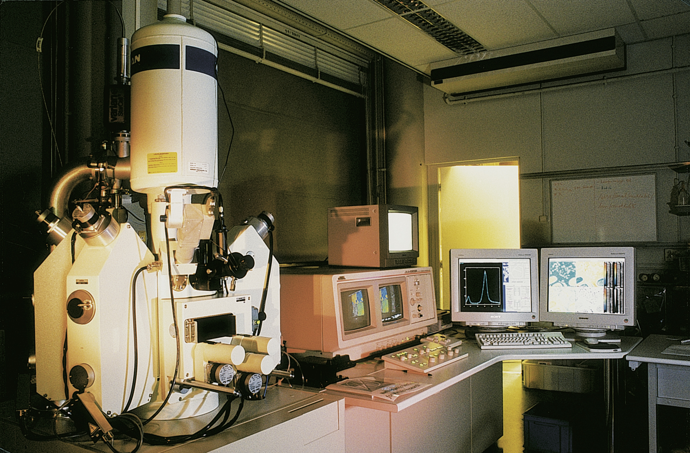
Electron Probe X-ray Micro Analyzer, EPMA (fully automated JEOL JXA 8900R WD/ED combined microanalyzer) equipped with five wavelength-dispersive (WD) spectrometers and one energy-dispersive (ED) system, which allow quantitative composition analysis of the elements in the range of 4Be to 92U. For the analysis of light elements (i.e. Be, B, C, N and O) the WD spectrometers are provided with 4 dedicated multilayer crystals. To mitigate surface contamination, this instrument is provided with an oil-free pumping system, an automated gas-jet and liquid nitrogen trap.
Scanning Auger Electron Spectroscopy
Scanning Auger Microprobe, AES/SAM (PHI 4300 SAM), equipped with a 5 keV ion-gun for depth profiling, a Quadrupole Mass Spectrometer (Pfeiffer QMS 422) for Secondary Ion Mass Spectroscopy and Zalar sample rotation for high resolution depth profiling.
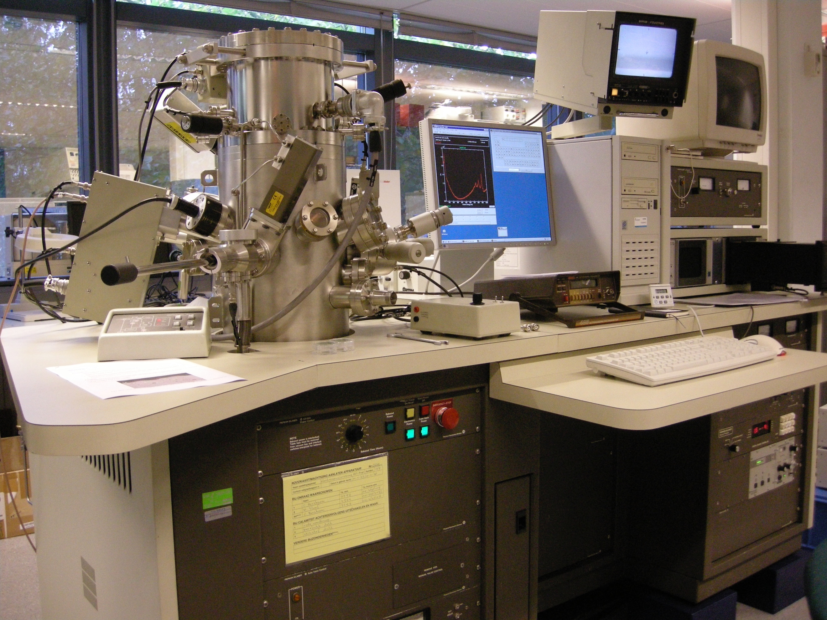
X-ray Photoelectron Spectroscopy
X-ray Photoelectron Spectrometer, XPS (PHI 5400 ESCA), equipped with a dual anode (Al/Mg) X-ray source and a 5 keV ion-gun for depth profiling and Zalar sample rotation for high resolution depth profiling. This system offers possibility of small area analysis and angle-resolved photoelectron spectroscopy.