KIC grant awarded to improve imaging of semiconductor chips
The Dutch Research Council (NWO) has awarded a grant to research on more efficient production of even smaller computer chips in the KIC call ‘Demand-driven Partnerships for Consortia’. Researchers from Delft University of Technology and ARCNL are collaborating with ASML in order to inspect computer chips more precisely and faster with help of electrons. The Knowledge and Innovation Covenant (KIC) research programme stands for pioneering innovative solutions with social and economic impact. NWO funds the research with almost 2 million euros, ASML contributes with over 2.3 million co-funding.
Chips are an indispensable element of any electronical system. They are composed of many tiny semiconductor components that are used in a variety of technologies, including computers and smartphones. Powerful semiconductors will have a vast influence on artificial intelligence, advanced networks (5G), healthcare, cars, the internet of things, and much more. Rapid, accurate and precise imaging during fabrication of the devices is essential for making smaller and thus more powerful devices. The continuing miniaturisation of semiconductor devices needs techniques that allow imaging the smallest details in these devices.
Smaller and more powerful chips
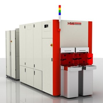
In this project, Jacob Hoogenboom and Kees Hagen from Delft University of Technology are working together with ARCNL and high-tech company ASML to achieve improved imaging of even smaller semiconductor components. By using electrons instead of light, the highest possible resolution can be achieved for visualising semiconductor components. However, electron imaging technology still has some shortcomings that limit its applicability and reliability for routine application. In this research project, the consortium partners aim to overcome these shortcomings. The knowledge gained from this project will lead to more precise and faster inspection during manufacturing and thereby to more efficient production of yet smaller semiconductor devices.
“ASML has had an excellent relationship with the academic world since its early years,” says Timon Fliervoet, system architect electron beam systems at ASML and guest researcher at TU Delft. “I am therefore very enthusiastic about this collaboration with TU Delft and ARCNL. When industrial engineering and fundamental science come together, meaningful innovations can emerge. At the same time, this collaboration offers the opportunity to work with and possibly attract talented PhD candidates.”

Jacob Hoogenboom, Associate Professor at the Department of Imaging Physics:
“Computer chips have become an integral part of today's society. By making their components smaller and smaller, computer chips have become increasingly powerful over the years. Emerging technologies such as artificial intelligence require even more powerful and, therefore, smaller chips. In addition, further downsizing can also make computer chips more energy efficient and thus sustainable.
A major challenge, however, is that the components in computer chips are already becoming so small that we can hardly make them visible and thus inspect them with conventional techniques based on light. Inspection with electrons offers a solution to this, though the technique still has major, fundamental shortcomings. For example, the throughput of inspection with electron microscopes is still far too low and exposure with electrons also leads to damage and artifacts that make it difficult to achieve a reliable image.
Together with ASML and our colleagues at ARCNL, we aim to obtain a better fundamental understanding of the processes that lead to damage and artifacts and use this understanding to arrive at faster and more reliable electron imaging.”

