Research collaboration | Faster and more reliable electron imaging
Item 1
van
1
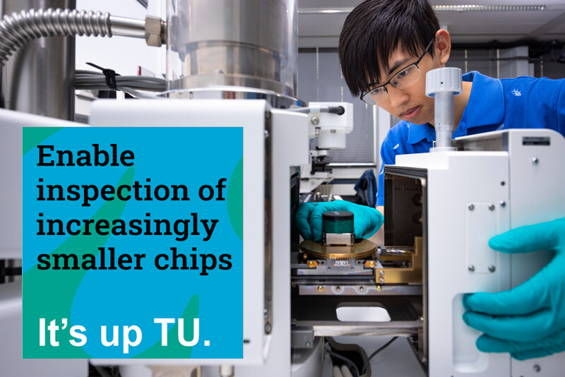
Pushing boundaries to inspect increasingly small computer chips
There is a growing demand for smaller and more powerful computer chips. A major challenge to meet this demand is that when components are extremely small, it is hard to make them visible and inspect with light. By using electrons instead of light, the highest possible resolution can be achieved for visualising semiconductor components. Inspection with electrons offers a solution, but the technique still has major, fundamental shortcomings.
ARCNL, Delft University and ASML will join forces to get a better understanding of the causes of current limitations enabling the realization of faster and more reliable electron imaging for the semiconductor industry.
The great thing about our research is that is combines fundamental physics with electronics, vacuum science, software development and instrument design
―
Kees Hagen,
Associate Professor TU Delft
ASML has had an excellent relationship with the academic world since its early years. I am therefore very enthusiastic about this collaboration. When industrial engineering and fundamental science come together meaningful innovations can emerge. By working together, we can push technologies to new limits, and it helps us to sustain our long term roadmap.
―
Timon Fliervoet,
System architect electron beam systems at ASML and guest researcher at TU Delft
Electron-induced effects and light-induced effects have a lot in common. We are looking forward to building a bridge between light-matter interaction, surface science, and electron microscopy together with our partners at ASML and TU Delft.”
ARCNL
Next generation Electron Imaging
To develop the next generation Electron Imaging we combine fundamental research with industrial engineering. For a first impression of our research team and laboratory in Delft watch the video below.