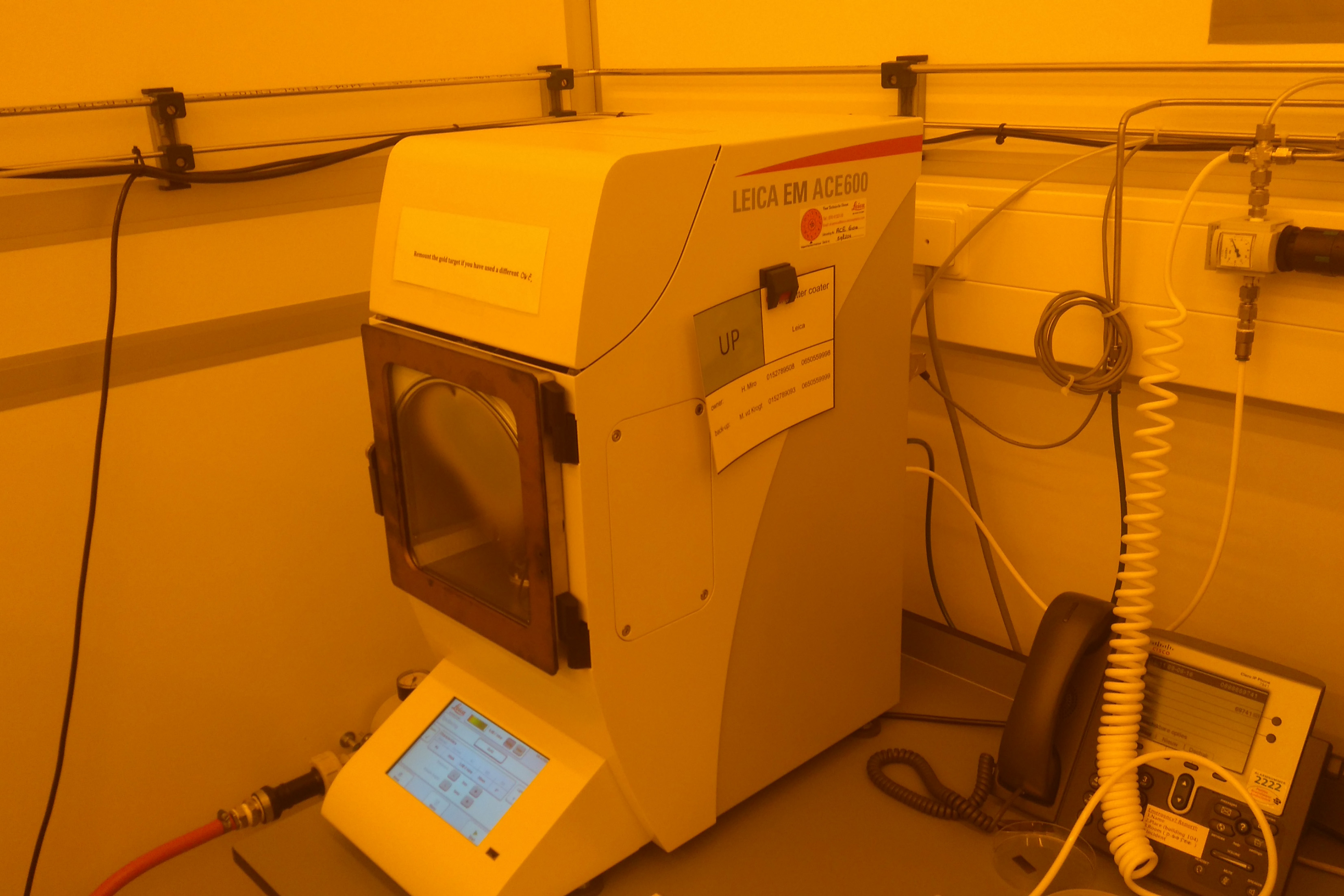
Leica EM ACE600
Apparatus |
| Leica EM ACE600 high vacuum sputter coater |
Supplier | Leica, www.leica-microsystems.com | |
Location | P00.550 | |
Main purpose | Coating samples with thin conductive films for SEM and TEM analysis | |
System layout | DC and RF magnetron sputter deposition (4x 4 inch target) RF sputter etching
| |
Gasses | Ar | |
Process information | Gold, Chromium, Platinum and gold/palladium. very fast, depositing a 10nm layer takes less than 10min including pumping and venting time.
| |
Facilities | Vacuum chamber, touch screen control panel, rotating sample stage, quartz (QSG) thickness measurement and sputter source. | |
Specimen | max. 100mm wafers, small pieces allowed | |
Equipment owner | Hozan Miro h.miro@tudelft.nl +31 650559998 Marco van der Krogt (back-up)m.c.vanderkrogt@tudelft.nl +31 650559999 |