Compass
The 25.6% world record c-Si solar cell is based on amorphous silicon passivating contact technology. However, base materials alternative to amorphous silicon exist for passivating contacts, which not only have comparable passivating and conductive properties, but also have other technological or industrial advantages, such as higher transparency or better thermal stability. In order to maintain a competitive edge in Dutch solar cell knowhow and equipment manufacturing, the goal of the COMPASS project is to explore, combine, and demonstrate high-performance and manufacturability of such novel, high-potential passivating contact materials that are being developed in the Netherlands. The project will result in know-how on the critical parameters of the developed passivating contact layers, both individually and combined in a solar cell with a targeted efficiency of 23%. Moreover, an inventory of the industrial applicability of the fabrication process of such a cell, based on cost and scalability, will be made.
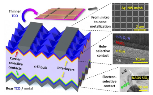
Example of the ‘moly-poly’ cell, a possible result of the COMPASS project: a solar cell with both contact polarities formed by novel passivating contacts. On the front side there is a passivating stack with MoOx as the hole-selective layer, covered by a thin layer of In2O3:H or PLD ITO and a Ag NW mesh for improved lateral conductivity. On the rear side there is a SiO2/n-type polysilicon stack covered with (optional TCO) and a full area metal contact.
Research objective
PVMD group brings in its expertise on passivating layers and integrating these layers in a working lab solar cell to evaluate the processes and to explore the efficiency limits of this cell design. The focus of the PVMD group is on materials and solar cell devices. (1) Develop n-type polysilicon layer and/or alternative electron-selective layers: The focus lies on the development of an n-type polysilicon contact as an electron-selective contact. Both in-situ and ex-situ doped polysilicon will be explored (in-situ via PECVD a-Si:H + crystallization + hydrogenation and ex-situ via LPCVD a-Si + implantation + crystallization). Although n-type polysilicon has been demonstrated to be very suitable as an electron-selective contact, but also various other new electron-collecting layers, such as TiO2, may be tested. (2) Patterning of passivating layers and metal contacts: An alternative to minimizing absorption at the front side of the solar cell is to place both contacts at the rear. However, patterning of the active layers is required for this purpose, which brings up new challenges. IBC test structures with the new layers will be made in this task. If the result looks promising and if the budget allows it then the tests will be extended to IBC solar cells.
Compass
Subsidy: TKI
Duration: 2016-2018
People involved: Dr. Olindo Isabella, Dr. Guangtao Yang

